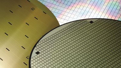
Back End Process
Achieve higher yields, enhanced traceability, and faster ROI with zero-defect quality chip production: Our combinable 2D and 3D analysis systems significantly improve quality assurance by inspecting all chips individually and evaluating the integrated circuit packaging. Integrated at the interface between the front-end and back-end, ISRA inspection systems detect defects in individual components at the wafer level and in the dicing frame. This 100% inspection ensures that only flawless material is sent to the customer.
Wafer Level Bonding
The downsizing of electronic devices is challenging semiconductor manufacturers to produce smaller component sizes while maintaining tighter process control requirements.
ISRA VISION's wafer inspection solutions for advanced wafer-level packaging ensure traceability throughout the semiconductor manufacturing process. Our systems provide superior quality control for improved device performance, enabling manufacturers to detect, resolve and monitor process deviations in a timely manner.
Benefits
- Efficiency: simultaneous scanning of the bulk wafer material, and the wafer edge
- Flexibility: seamless integration into existing process lines
- Increased uptime: minimize wafer breakage during processing
- Features
- Typical defects
- Technical data
- Reliable defect detection and classification
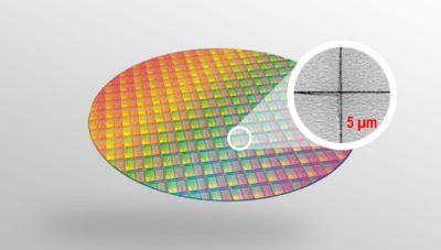
- Defect detection down to <5 µm crack width
- Wafer mapping / 2D coordination map
- Throughput: up to 180 wph
- Edge inspection tool integrated into pre-aligner
- Microcracks inside the bulk wafer material
- Edge chippings
- Cracks near edge
- Edge contaminations
- High-resolution line scan cameras with LED line illumination using different wavelengths
- Integrated adjustment of thresholds and crack characteristics for sensitive optimization of the detection result
- Typ. resolution: 20 μm, optional down to 1.5 μm
- Semi standard interface
Download additional information

CrackScan brochure en
- Filename
- brochure-crackscan-semiconductor-en.pdf
- Größe
- 311 KB
- Format
- application/pdf
 test123
CrackScan brochure cn
- Filename
- brochure-crackscan-semiconductor-cn.pdf
- Größe
- 488 KB
- Format
- application/pdf

EdgeScan brochure en
- Filename
- brochure-edgescan-semiconductor-en.pdf
- Größe
- 464 KB
- Format
- application/pdf

EdgeScan brochure cn
- Filename
- brochure-edgescan-semiconductor-cn.pdf
- Größe
- 523 KB
- Format
- application/pdf
Re-Thinning
Re-thinning can introduce defects on the wafer's surface that can impact the performance and functionality of the final semiconductor device.
Therefore, optical inspection after re-thinning is crucial to detect defects that could impact device functionality.
Conducting optical inspection after the re-thinning process allows manufacturers to minimize the risk of defects and ensure that the final semiconductor devices meet the required performance and reliability standards. This helps to enhance the overall quality and yield of the semiconductor manufacturing process.
Benefits
- Efficiency: simultaneous scanning of bulk and surface at line speeds of up to 180 wafers/hour
- Flexibility: seamless integration into existing process lines
- Increased uptime: minimize wafer breakage during processing
- Customized, seamless integration into wafer handling solutions
- 100% control of the re-thinned wafer edge in parallel to other process steps - no influence on existing cycle times
- Features
- Typical defects
- Technical data
- Reliable defect detection and classification
- Defect detection down to <5 µm crack width
- Wafer mapping / 2D coordination map
- Process control of cracks/chip-outs at the re-thinned wafer edge
- Throughput: up to 180 wph
- Edge inspection tool integrated into pre-aligner
- Microcracks inside the bulk wafer material
- Edge chippings
- Cracks near edge
- Contaminations
- High-resolution line scan cameras with LED line illumination using different wavelengths
- Integrated adjustment of thresholds and crack characteristics for sensitive optimization of the detection result
- Typ. resolution for microcrack inspection: 20 μm, optional down to 1.5 μm
- Pixel resolution for edge inspection: typ. 3 μm/px
- Integration with thin wafer handling
- Semi standard interface
Download additional information
CrackScan brochure en
- Filename
- brochure-crackscan-semiconductor-en.pdf
- Größe
- 311 KB
- Format
- application/pdf
test123
CrackScan brochure cn
- Filename
- brochure-crackscan-semiconductor-cn.pdf
- Größe
- 488 KB
- Format
- application/pdf
EdgeScan brochure en
- Filename
- brochure-edgescan-semiconductor-en.pdf
- Größe
- 464 KB
- Format
- application/pdf
EdgeScan brochure cn
- Filename
- brochure-edgescan-semiconductor-cn.pdf
- Größe
- 523 KB
- Format
- application/pdf
Post-Dicing Inspection
Dicing wafers carries the risk of defects in the dicing streets. Accurate inspection of the dicing street reliably detects these defects and minimizes the scrap rate of chips and dies. The DicingScan inspection tool provides 100% wafer inspection. High-performance line scan cameras precisely detect defects such as edge chippings in the dicing streets. In addition, the tool checks the presence, position, and completeness of the dicing streets.
With our patented MultiView imaging technology, which forms the basis of the WafQScan process, users can also inspect the rear side of the wafer through the carrier tape (foil). DicingScan ensures that only dies/chips of impeccable quality are processed.
Benefits
- Efficiency: Multiple inspection tasks in one scan
- 100% quality control: Only high-quality dies and chips are processed
- Features
- Typical defects
- Technical data
- Dicing street inspection immediately after dicing
- (Micro-)crack inspection on dies
- Check the position, integrity, and quality of dicing strees
- Front and rear side inspection, even through the carrier tape
- Uncompleted dicing
- Cracks
- Bubbles
- Releases
- Chip-outs
- MultiView technology with simultaneous image capturing
- Semi standard interface
Production Analytics
Die webbasierte Production Analytics Plattform ermöglicht es Ihnen, den Systemstatus aller Produktionslinien auf einen Blick zu überprüfen oder Produktionsdaten im Detail zu analysieren.
Mit dem Qualitätsmanagementsystem analysieren Sie historische Daten, überwachen aktuelle Prüfdaten in Echtzeit und ermitteln zukünftige Trends in Ihrem Produktionsprozess.
Optimierung der Produktion
Über Dashboards können Sie die Daten der Produktionslinie und des Produkts vor Ort oder von unterwegs aus vergleichen und erhalten so wichtige Erkenntnisse für die Optimierung. So treffen Sie fundierte Entscheidungen entlang Ihrer Wertschöpfungskette, um die Produktqualität und die Rentabilität zu steigern. Die Fortschritte der Optimierungsmaßnahmen können Sie kontinuierlich verfolgen und mit visualisierten, erweiterten Berichten darstellen.
Frühzeitiges Erkennen von Produktionsfehlern
Grenzwertüberschreitungen können Sie in jedem Produktionsschritt, mithilfe von Live-Statusinformationen und automatischen Warnmeldungen schnell erkennen und deren Ursache finden. Damit lösen Sie Produktionsfehler schnell, verkürzen Ausfallzeiten und senken die Produktionskosten.
Vorausschauende Wartung
Potenzielle Anlagenausfälle können Sie durch die Analyse von Echtzeitdaten aus den Sensoren und Überwachungssystemen verhindern. Dies ermöglicht eine proaktive Planung der Wartung, die auf dem tatsächlichen Zustand der Maschinen basiert, anstatt einem festen Zeitplan zu folgen. Dieser datengestützte Ansatz spart Kosten durch geringere Ausfallzeiten und erhöht die Gesamtproduktivität sowie die Lebensdauer der Produktionslinie.
Ihre Vorteile
- Zeitsparende mehrzeilige Übersichten, eine Ansicht für alle qualitätsbezogenen Informationen
- Minimierung von Ausfallzeiten durch Überwachung der Systemzustandsdaten
- Schnellere Reaktion auf Qualitätsprobleme durch Überwachung der Qualitätsdaten
- Schnelle Beseitigung von Produktionsfehlern, Reduzierung der Produktionskosten
- Verbesserte Wartung für geringere Ausfallzeiten, höhere Gesamtproduktivität und längere Lebensdauer der Produktionslinie
Funktionen
- Überblick über Produktionsdaten und Anlagenstatus
- Webbasierte Lösung, keine Installation von Client-Software erforderlich
- Abteilungsbezogene Dashboards, kundenspezifische Anpassungen sind möglich
- Live-Einblicke aus Echtzeitdaten
- Offen für die Integration relevanter Drittdaten und den Export von Daten in die Systeme des Kunden
- Schwellenwertüberwachung und Alarmierung
Servicelösungen und Schulungen


Für den effizienten und zukunftssicheren Betrieb Ihrer Produktionsanlagen unterstützen Sie unsere hochqualifizierten Serviceteams weltweit in allen Belangen. Wir übernehmen die Implementierung, Wartung und Instandhaltung sowie die Analyse und Optimierung Ihrer Anlagen.
Lernen Sie in der ISRA VISION Academy, wie unsere kompetenten Trainer Ihre Mitarbeiter immer auf dem neuesten Stand des Wissens halten, damit Anlagenbediener, Produktingenieure und Qualitätsmanager zu echten Inspektions-Experten werden.